Introduction
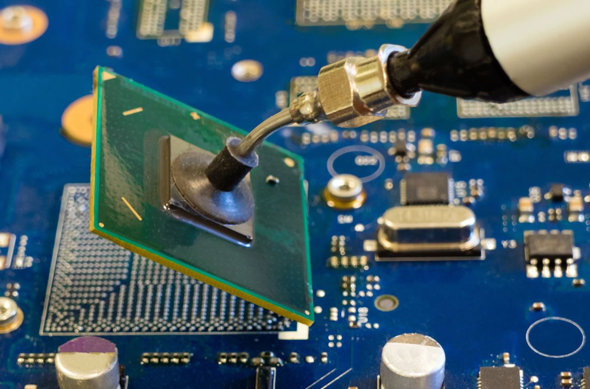
Soldering is a fundamental process in electronic assembly, allowing components to be securely attached to printed circuit boards (PCBs). However, the high temperatures involved in soldering can subject PCBs to thermal stress, potentially leading to issues such as warping, delamination, and component failure. Minimizing thermal stress during soldering is crucial to ensure the reliability and performance of electronic devices. In this article, we will explore techniques and best practices to minimize thermal stress on PCBs, supported by existing technologies and real-world examples.
I. Understanding Thermal Stress in Soldering
1.1 The Impact of Thermal Stress
During soldering, PCBs are subjected to rapid temperature changes, which can cause the materials to expand and contract unevenly. This thermal stress can result in mechanical and structural issues that compromise the integrity of the PCB and its components.
1.2 Factors Influencing Thermal Stress
Several factors contribute to thermal stress during soldering. The size and thickness of the PCB, the components’ thermal characteristics, the soldering process parameters, and the materials used all play a role in determining the level of thermal stress experienced by the PCB.
1.3 Real-World Example: Lead-Free Soldering
The introduction of lead-free soldering, mandated by environmental regulations, has posed additional challenges in minimizing thermal stress. Lead-free soldering requires higher temperatures, increasing the risk of thermal stress on PCBs. Therefore, implementing effective strategies to mitigate thermal stress is crucial in lead-free soldering processes.
II. Design Considerations for Thermal Stress Minimization
2.1 Thermal Relief Patterns
Thermal relief patterns, such as copper planes or thermal spokes, can be incorporated into PCB designs to reduce the impact of thermal stress. These patterns allow for better distribution of heat during soldering, minimizing the differential expansion and contraction of materials.
2.2 Component Placement and Layout
Careful component placement and layout considerations can also contribute to minimizing thermal stress. Grouping high-heat-generating components together, optimizing component density, and ensuring sufficient spacing between components can help mitigate the concentration of heat and minimize thermal stress.
2.3 Real-World Example: HDI PCBs
High-Density Interconnect (HDI) PCBs, commonly used in smartphones and other compact devices, require special attention to minimize thermal stress. Their smaller size and higher component density make thermal management critical. Advanced design techniques, such as microvias and buried vias, allow for better heat dissipation and reduced thermal stress on HDI PCBs.
III. Soldering Techniques for Thermal Stress Reduction
3.1 Preheating and Controlled Heating Rates
Preheating the PCB before soldering and utilizing controlled heating rates can minimize thermal shock and reduce thermal stress. Gradual heating allows the PCB materials to expand more uniformly, reducing the strain caused by rapid temperature changes.
3.2 Reflow Profiles and Temperature Optimization
Optimizing reflow profiles and temperature settings is crucial in minimizing thermal stress. Understanding the specific requirements of solder paste, components, and PCB materials allows for the establishment of reflow profiles that achieve proper soldering while minimizing the impact of thermal stress.
3.3 Real-World Example: Vapor Phase Soldering
Vapor phase soldering is a soldering technique that can help reduce thermal stress. In vapor phase soldering, the PCB is immersed in a vapor of a heat transfer fluid with a known boiling point. The controlled heat transfer from the vapor to the PCB ensures uniform heating and minimizes thermal stress during soldering.
Conclusion
Minimizing thermal stress on PCBs during soldering is crucial for ensuring the reliability and performance of electronic devices. By understanding the factors contributing to thermal stress, implementing appropriate design considerations, and utilizing soldering techniques that mitigate thermal stress, manufacturers can minimize issues such as warping, delamination, and component failure. Real-world examples, such as the challenges posed by lead-free soldering and the considerations for HDI PCBs, demonstrate the importance of addressing thermal stress in diverse applications. As technology continues to advance, it is essential to stay updated on the latest techniques and technologies to effectively minimize thermal stress and ensure the long-term reliability of electronic devices.


